
Print Circuit Boards (PCBs) are at the heart of most modern electronics, including industrial machines, antennas, and smart systems. Ensuring PCB performance is paramount for successful product or systems design. However, ever increasing demands for more versatile functions, higher speeds, and smaller footprints pose significant challenges to the design of the PCB.
The component and signal trace density increase of today’s PCBs is making the digital simulation and analysis of their electromagnetic (EM) performance a must to save on costly redesign cycles. This makes simulation software a key part of the PCB designer’s toolbox for effective and efficient design. With its multi-solver capabilities, CST Studio Suite EM simulation software allows designers to identify potential performance issues early in the design stage. Users can virtually test various operational environments, optimize the design, and ensure PCB functionality and reliability from component to system level before prototypes are built.
In this blog, we’ll look at the CST Studio Suite EM technology that enables a comprehensive simulation approach, analyzing different aspects of PCB design: signal and power integrity (SI/PI) and electromagnetic compatibility (EMC).
File Types and Formats Supported by CST Studio Suite
CST allows various file types to be imported for PCB analysis, including 2D or EDA files and 3D CAD files. It also supports numerous EDA file formats, including Gerber, Cadence, Mentor Expedition/Hyperlynx, ODB++, and Zuken.
Signal and Power Integrity Performance of PCB
When PCB boards are designed, they need to meet certain specifications. For example, signals sent from one end of the transmission line to the other need to retain a certain shape. In other words, the electrical signals need to maintain a certain quality. This is referred to as signal integrity.
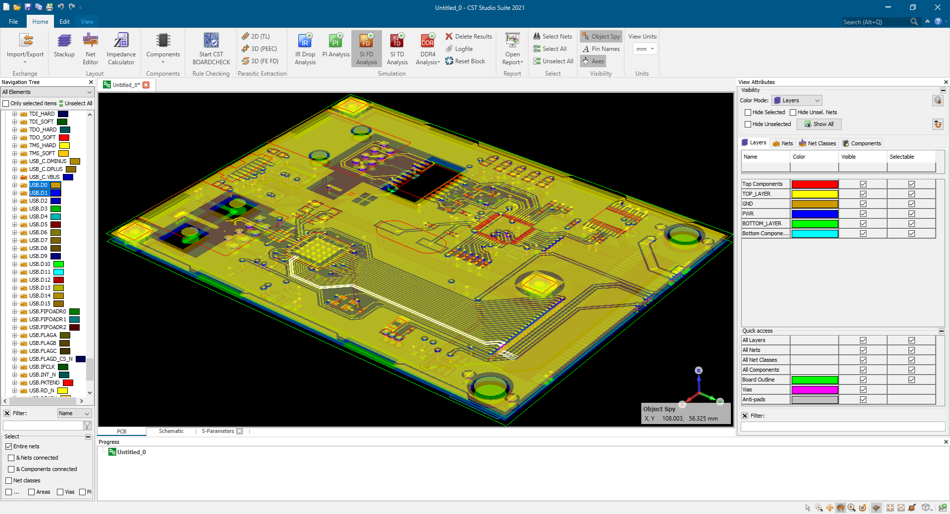
In CST, the EDA files can be analyzed in different ways, depending on what result is of interest. If signal integrity, power integrity and IR-Drop performance are required, then CST’s PCB Studio (PCBS) can be used. With this application-specific module, users have the ability to control what type of data to import: layout geometry, stackup data, component-to-part mapping, and component models.
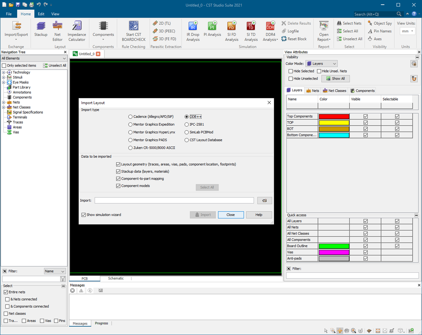
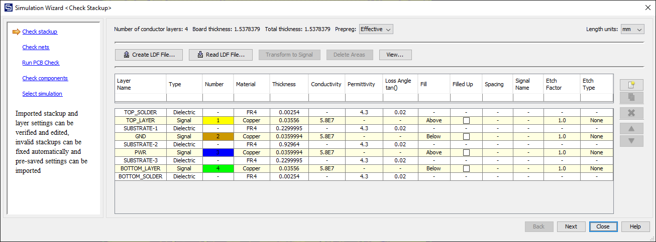
The image above shows the PCBS EDA import interface for the various formats supported. The simulation wizard is automatically opened after the file is selected. It allows users to view the stackup information and change layer thickness, etch factor, and etch type under the check stackup stage. Net class and net specifications can be specified in the Check nets stage.
Modifications to the stackup can be made and saved to an LDF file for later use. Components can be edited, for example, capacitors can be specified as standard model where the capacitance, parasitic resistance and parasitic inductance can be entered. If measurement data in the form of TOUCHSTONE is available, the component can be defined using such TOUCHSTONE file. Vendor model SPICE-subcircuits can be used if it exists in the model library.
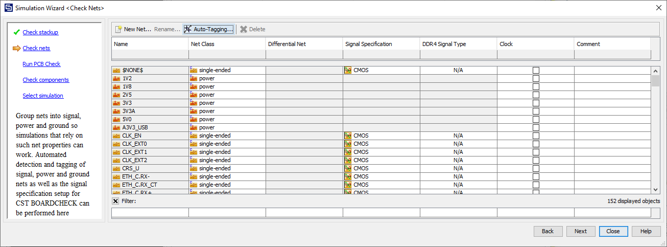
The nets can be tagged properly using the Auto-Tagging feature, which allows for easy assignment of the net classes by entering specific net name conventions. Signal specifications can be defined by selecting the nets using the same technology.
The imported EDA file can be visualized using the built-in 3D viewer. Many solvers are embedded in PCBS. In the 2021 version of CST Studio Suite, an additional DDR4 analysis option is available. It is implemented as a Wizard for signal integrity analysis based on DDR4 technology.
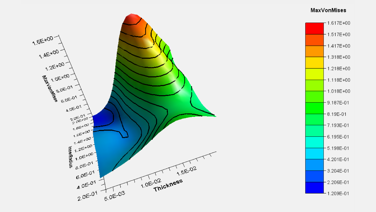
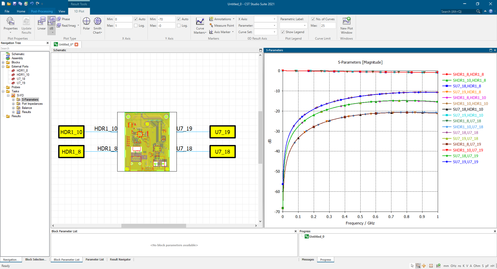
An analysis of the signal integrity in the frequency domain (S-Parameters) is shown below. This was done with a few button clicks after defining the I/O devices.
EMC Performance of PCB Using 3D Simulation
The above simulation approach is strictly for PCB performance analysis without radiation taken into account. For full wave simulation, including EMC testing, users can convert the EDA file into a 3D geometry and analyze it using CST Microwave Studio (MWS) and the built-in converter. Note that it is also possible to convert the PCB into 3D geometry directly in PCBS.
The interface below shows the MWS EDA import process.
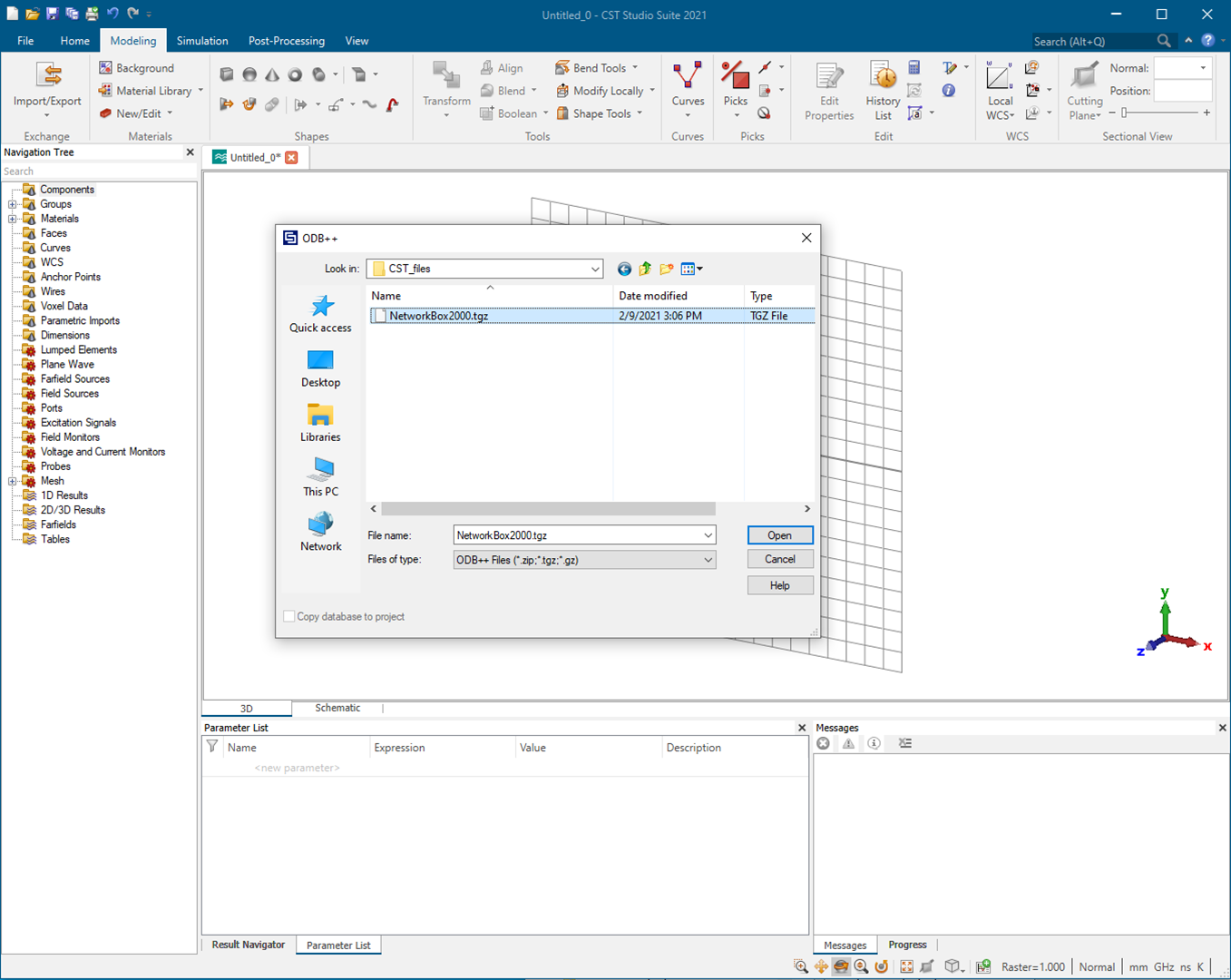
The associated lumped elements – resistors, inductors, and capacitors – will be imported and created automatically. It is also possible to define excitation ports directly in the EDA import dialog.
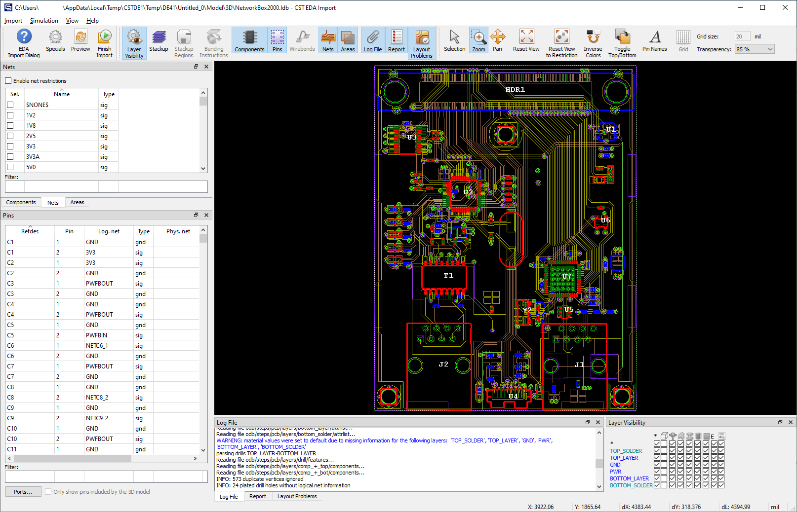
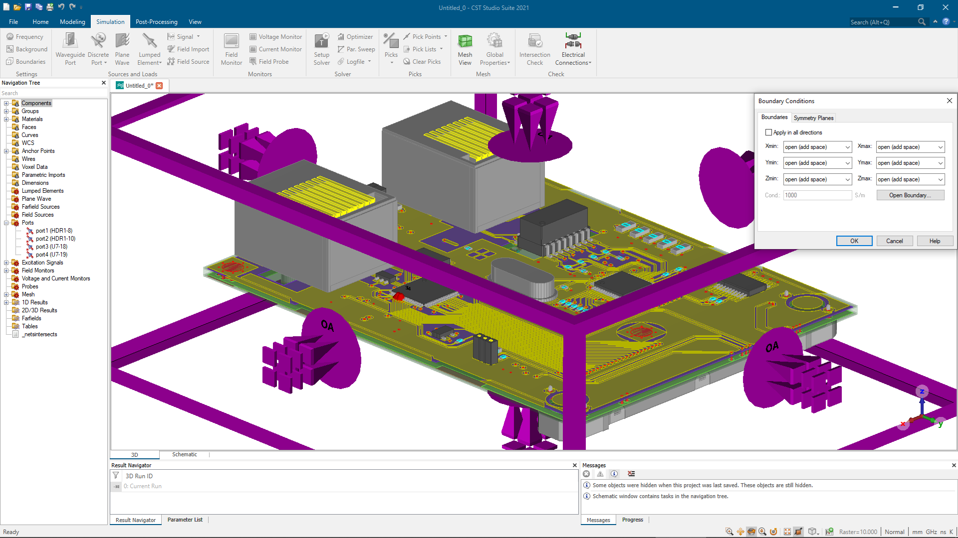
Once the EDA file is set up properly, users can run the 3D EM simulations. The 3D CAD models like the connectors, pins and components can be visualized in 3D similar to the signal integrity approach . The excitation, frequency range, background material, and boundary conditions need to be set appropriately. With 3D geometry, users can choose the appropriate solver for the simulation. The general-purpose time domain solver and frequency domain can be used depending on the model size and frequency range.
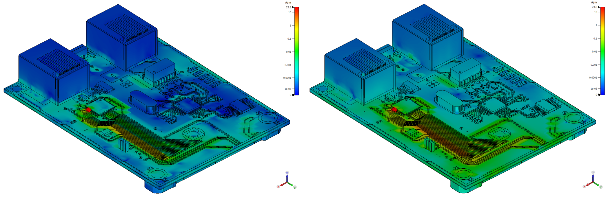
One of the biggest advantages of 3D simulation is the ability to visualize the field distribution to gain additional insight. Physical EMC measurements give you a pass/fail result but do not provide further information as to why the device passed or failed the test. For example, simulation allows you to study the magnetic field distribution within the context of the design, enabling you to re-route the traces differently to minimize the unwanted magnetic field. The following comparison shows the magnetic field distribution between a differential excitation with and without delay.
For more information on what licensing configuration is used in this analysis, please send us an email at info@inceptra.com.
Complete EM Simulation Technology in One License
The standard CST Studio Suite license includes all solvers, making it possible for you to perform different types of electromagnetic simulation for a complete analysis approach to ensure PCB functionality. The powerful all-in-one tool features a streamlined interface and easy transitions between problem types, facilitating learning.
For this blog, we used the same EDA file for different simulations:
- CST PCB Studio for the quick computation of the PCB signal integrity or power integrity, an efficient way to assess performance for the traces of interest;
- CST Microwave Studio to convert the EDA file into a 3D CAD model for full wave simulation, taking all coupling effects into account, to virtually test for EMC.
Questions?
If you have any questions or would like to learn more about CST Studio Suite electromagnetic simulation software solutions for PCB analysis, contact us at (954) 442-5400 or submit an online inquiry.